The complete guide to PCB pad :types, size, spacing, repair and comparison - IBE Electronics
5 (106) In stock

Soldering is one of the most important processes in PCBA processing. On printed circuit boards, electrical connections to all components are made via PCB pads. The PCB pads are a very critical part of the PCB that determines where components are soldered on the PCB.The size, shape, and position of pads in a PCB directly depend on the manufacturing quality of the board. Today we will take a look at the PCB pad in SMT soldering.
Soldering is one of the most important processes in PCBA processing. On printed circuit boards, electrical connections to all components are made via PCB pad.
What is a Pad in PCB Design and Development

Solved Nep AutoZone Produces Brake Pads Using A Standard, 45% OFF

The complete guide to PCB pad :types, size, spacing, repair and comparison - IBE Electronics
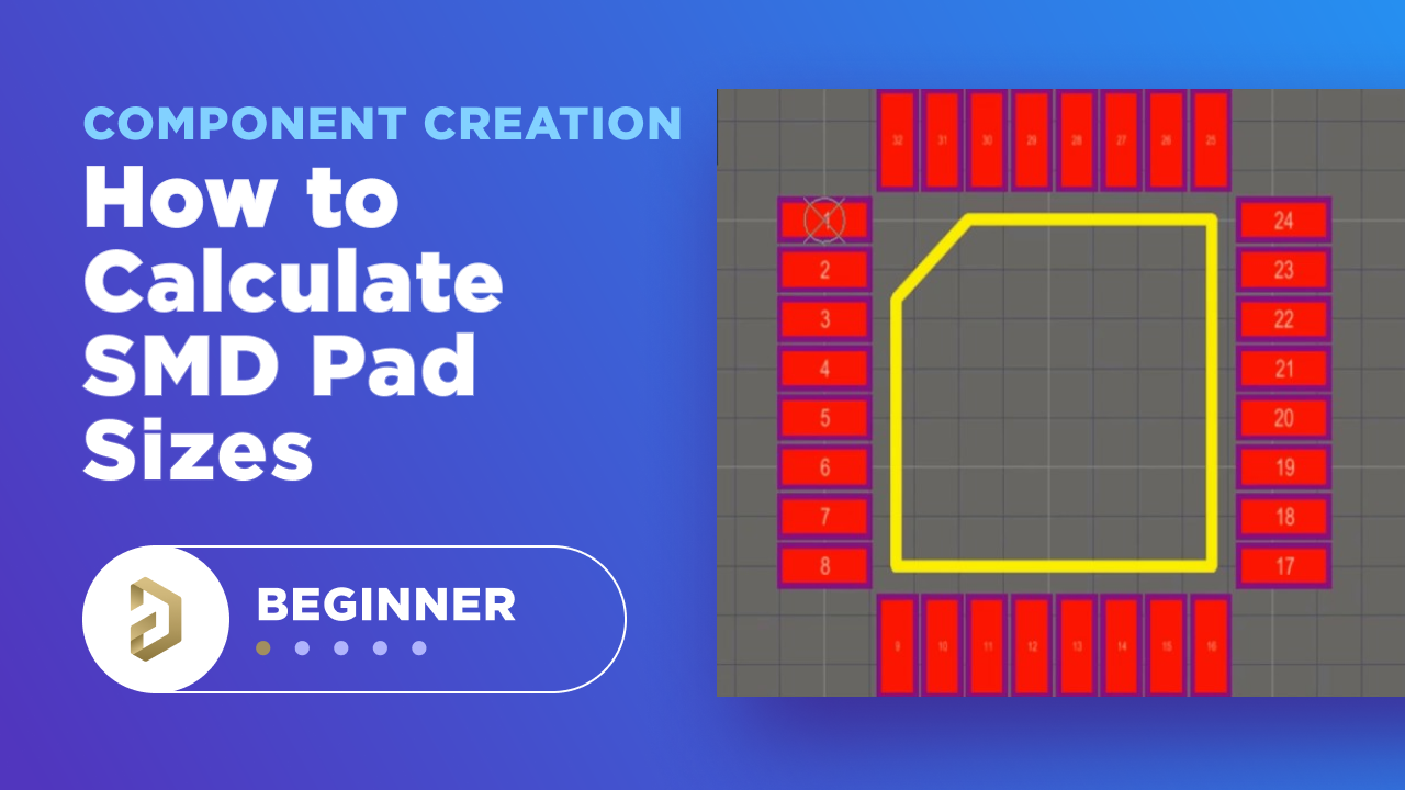
Best Methods for Calculating SMD Pad Size in PCB Design

Several details that are usually neglected about PCB vias - IBE Electronics
List of Tools Needed for PCB Rework
PCB Manufacturing Process – A Step by Step Guide

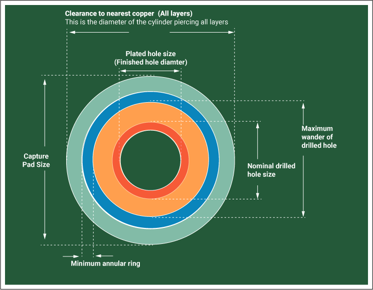
PCB Pad Size Guidelines: Finding the Proper Pad Sizes for Your Circuit Design
PCB Basics - SparkFun Learn
How to scale margin and padding with @ScaledMetric Property Wrapper
Smart Batching Tutorial - Speed Up BERT Training · Chris McCormick
a) Traditional WDM networks with fixed spacing grid (50GHz); (b)


:max_bytes(150000):strip_icc()/tatchabrandreview-e04e62cf84bd458d871ad55a6b69aff1.jpg)
