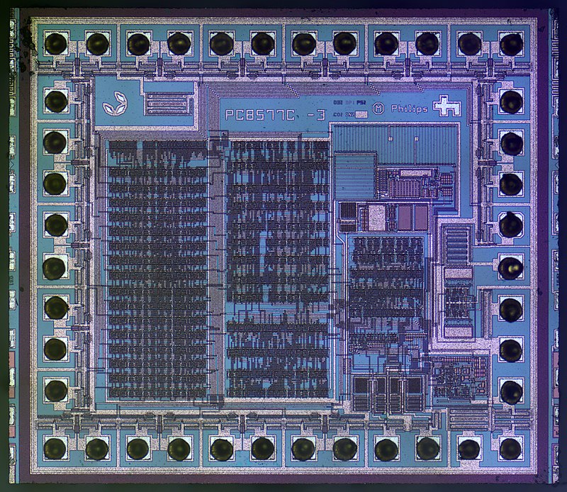
Details of test chip designs: pad pitch, layout, materials, and opening.
4.5 (246) In stock

Integrated circuit - Wikipedia
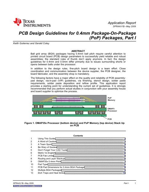
PCB Design Guidelines for 0.4mm Package-On - Texas Instruments
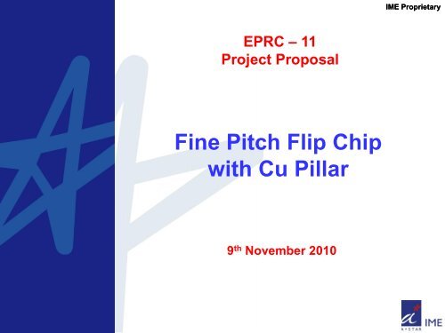
Fine Pitch Flip Chip with Cu Pillar

What is a Pad in PCB Design and Development
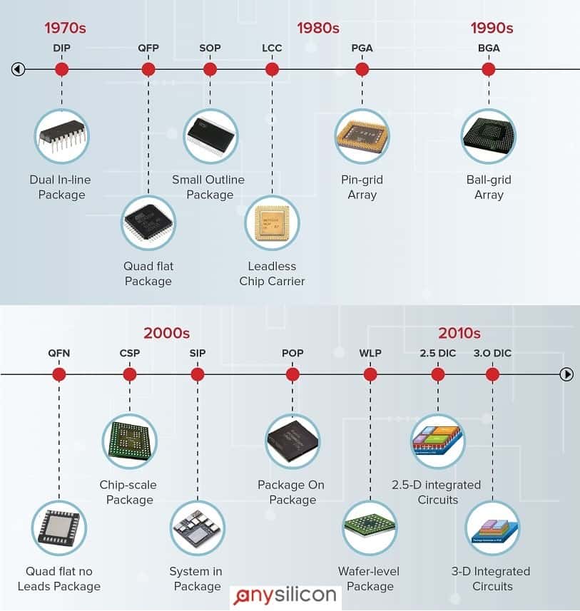
The Ultimate Guide to Semiconductor Packaging - AnySilicon

Shifting Left for Earlier Testing in 2.5D and 3D IC Design

PCB pad design principles

Introduction of Plastic Ball Grid Array (PBGA) - FS PCBA
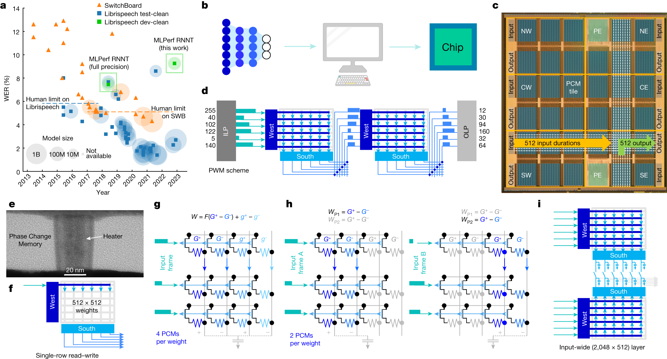
An analog-AI chip for energy-efficient speech recognition and transcription

Top PCB Layout Recommendations for BGA Packages

Automated fabrication of hybrid printed electronic circuits

Pad Stack Design And Fine Pitch Components, Part 2
🔴 O XIAOMI REDMI PAD TEM ENTRADA PARA CHIP?
Realme Pad 2 is official - 11.5 120Hz display, Helio G99 chip - news
App note: Exposed pads on some IC packages – Dangerous Prototypes
 SHAPERX Shapewear for Women Tummy Control Bodysuit Mid Thigh Butt Lifter Body Shaper Shorts,SZ5218-2-Black-2XL/3XL in Saudi Arabia
 Girls Camo Print Faux-Fur Lined Legging – Urban Planet
 Lace Up Corset Top Blouse Women Sexy Bustier Corset for Slimming
 The Benefits of Compression Stockings - Adaptive Technologies Inc.
 Red & White Nails With Black Leaves Gift for Her Women's Nails
 RYRJJ Men's Short Sleeve Button Up Linen Shirts Summer Casual Pocket Beach Dress Shirts(Brown,XL)